How Much Does It Cost to Build a CPU? Fab Construction & Financing Guide
Discover how much it costs to build a CPU in 2026. We break down semiconductor fab construction costs, cleanroom financing, and EUV tooling capital.

The True Cost of Silicon: Beyond Software and Design
When industry analysts and investors ask, how much does it cost to build a cpu, the answer extends far beyond software architecture, logic design, and Electronic Design Automation (EDA) licensing. In 2026, bringing a next-generation 2-nanometer (2nm) or 1.4nm CPU to market requires an estimated $20 billion to $30 billion in total capital expenditure (CapEx). While R&D and intellectual property account for roughly $1 billion to $1.5 billion, the lion's share of the cost is rooted in heavy physical construction and equipment financing. Building the semiconductor fabrication plant (fab) and the ultra-specialized cleanrooms required to manufacture the CPU represents the most expensive and complex commercial construction sector on the planet.
For construction estimators, facility financiers, and commercial real estate developers, understanding the capital stack of a CPU requires analyzing the intersection of mega-project civil engineering, microscopic environmental controls, and global equipment supply chains. According to the Semiconductor Industry Association (SIA), the capital intensity of semiconductor manufacturing now surpasses that of aerospace and traditional heavy industry, demanding entirely new paradigms for project financing and risk mitigation.
Deconstructing the Capital Stack: Where the Billions Go
To accurately estimate the cost to build a CPU, we must separate the physical facility construction from the tooling and operational ramp-up. Below is the standardized CapEx breakdown for a modern tier-1 logic fab (e.g., TSMC, Intel, Samsung) operating at the 2nm node in 2026.
| CapEx Phase | Estimated Cost Range (USD) | % of Total Budget | Primary Cost Drivers |
|---|---|---|---|
| Site Prep & Civil Shell | $1.5B - $2.5B | 10% | Land acquisition, waffle slab foundations, seismic isolation, structural steel. |
| Cleanroom & MEP Fit-Out | $3.5B - $5.0B | 20% | ISO Class 1 cleanrooms, Ultra-Pure Water (UPW), bulk gas delivery, HVAC. |
| Tooling & Lithography | $12.0B - $18.0B | 65% | High-NA EUV machines, deposition tools, etching, metrology. |
| Automation & Software | $500M - $1.0B | 3% | Overhead hoist transport (OHT), AI yield management, digital twins. |
| Ramp-up & Contingency | $500M - $1.5B | 2% | Scrap silicon, yield optimization, construction delay contingencies. |
The Physical Construction: Engineering a Mega-Fab
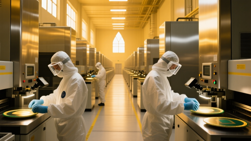
The physical shell of a CPU fab is a masterclass in extreme tolerances. A standard logic fab requires between 1 million and 1.5 million square feet of cleanroom space. However, this is not standard commercial cleanroom construction; it requires ISO Class 1 certification, meaning the air contains fewer than 10 particles sized 0.1µm or larger per cubic meter. Constructing these environments costs between $2,000 and $3,500 per square foot, vastly exceeding the $400-$800 per square foot typical of advanced biopharmaceutical facilities.
⚠️ Critical Construction Spec: Vibration Isolation
At the 2nm node, the features etched onto a silicon wafer are smaller than a strand of DNA. A passing truck or minor seismic tremor miles away can ruin a multi-million-dollar batch of CPUs. Fabs must be built on massive waffle slab foundations utilizing isolated pedestals that meet VC-F or VC-G micro-vibration criteria (vibration velocities below 1.56 µm/s). This requires pouring hundreds of thousands of cubic yards of specialized low-shrink concrete, decoupled from the facility's main structural columns to prevent acoustic transmission.
MEP Systems: The Hidden Cost Drivers
Mechanical, Electrical, and Plumbing (MEP) systems account for the majority of the facility construction budget. A single mega-fab consumes as much electricity as a mid-sized city (often requiring dedicated 300MW+ on-site substations) and processes millions of gallons of water daily.
- Ultra-Pure Water (UPW): UPW systems require multi-stage reverse osmosis, vacuum degasification, and electrodeionization. A UPW plant capable of producing 100,000 gallons per minute costs upwards of $150 million to construct.
- Bulk & Specialty Gases: CPUs require exotic gases like tungsten hexafluoride and neon. The construction of automated, double-walled bulk gas yards with redundant safety scrubbers adds $200M+ to the MEP budget.
- Thermal Management: Extreme UV (EUV) lithography machines generate massive heat loads. Dedicated chiller plants with redundant N+1 configurations are required to maintain ambient cleanroom temperatures at exactly 22°C (±0.1°C).
Financing the Unfinanceable: Capital Structures for Fabs
Because the cost to build a CPU ecosystem routinely exceeds $25 billion, no single corporation finances these projects entirely through free cash flow. According to SEMI, global fab construction spending has forced the industry to adopt complex, multi-layered financing structures. In 2026, a typical mega-fab is funded through a combination of the following mechanisms:
- Government Subsidies & Grants: Programs like the CHIPS for America program provide direct capital injections (often covering 15% to 25% of the facility construction cost) to onshore critical infrastructure.
- Investment Tax Credits (ITC): In the US, the 25% ITC for qualified semiconductor manufacturing property significantly offsets the tax burden on tooling and cleanroom MEP investments.
- Customer Advance Payments: Hyperscalers and fabless designers (e.g., Apple, Nvidia, AMD) frequently pre-pay billions of dollars for guaranteed future wafer capacity. This non-dilutive capital is used directly to finance the procurement of long-lead-time ASML lithography tools.
- Syndicated Debt & Sovereign Wealth: The remaining balance is typically covered by syndicated corporate debt facilities backed by consortiums of global banks, or joint-venture equity injections from sovereign wealth funds seeking domestic tech sovereignty.
Tooling Amortization and the ASML Monopoly
While construction estimators focus on the building, financiers must grapple with the equipment housed inside. The undisputed bottleneck in CPU manufacturing is the ASML High-NA EUV (Extreme Ultraviolet) lithography machine. In 2026, a single High-NA EUV unit costs approximately $380 million, weighs 150 tons, and requires a dedicated, climate-controlled sub-chamber within the cleanroom. A high-volume fab requires 10 to 15 of these machines. The financing of these tools requires specialized equipment leasing agreements and accelerated depreciation schedules, as the tools become technically obsolete within 5 to 7 years.
Decision Framework: Greenfield vs. Brownfield Fab Construction
When estimating costs and structuring debt, developers must choose between Greenfield (new build) and Brownfield (retrofit) construction. Each presents distinct financial and engineering profiles.
| Criteria | Greenfield Mega-Fab | Brownfield Retrofit / Expansion |
|---|---|---|
| Total CapEx | $20B - $30B+ | $8B - $14B |
| Timeline to First Silicon | 36 - 48 Months | 18 - 24 Months |
| Seismic / Vibration Control | Custom waffle slabs, optimal VC-G isolation. | Limited by existing foundation; requires active dampening retrofits. |
| MEP Integration | Purpose-built UPW and bulk gas yards. | Constrained by legacy pipe routing; requires modular skid solutions. |
| Financing Profile | Heavy reliance on government subsidies and long-term syndicated debt. | Often financed via internal CapEx budgets and equipment leasing. |
Risk Mitigation in Semiconductor Construction
The primary risk in financing CPU fabrication is schedule delay. A six-month delay in cleanroom certification can result in billions of dollars in lost revenue and breached customer supply agreements. To mitigate this, general contractors utilize modular cleanroom construction. By fabricating ISO Class 1 cleanroom cassettes, fan filter units (FFUs), and MEP racks in off-site controlled environments, contractors can reduce on-site assembly time by 30% and minimize particulate contamination during the build phase.
Ultimately, answering how much it costs to build a CPU requires looking past the silicon and staring directly at the concrete, steel, and ultra-pure plumbing that makes atomic-scale engineering possible. As node sizes shrink and EUV tooling costs rise, the construction and financing of semiconductor facilities will remain the most capital-intensive endeavor in modern industrial history.
Written by
Elena RodriguezElena Rodriguez is a civil engineer and technical writer specializing in concrete technology, masonry systems, and ASTM/ACI compliance. She earned her B.S. in Civil Engineering from Texas A&M University and spent a decade at a materials testing laboratory, performing over 2,000 concrete compressive strength tests and masonry prism evaluations. Elena is an ACI-certified Field Testing Technician (Grade I) and a member of ASTM Committee C12 on Natural Building Stone. She currently consults on forensic engineering cases involving concrete failures and moisture intrusion. Based in San Antonio, TX, Elena is a proud member of the Society of Women Engineers (SWE) and coaches her daughter's FIRST Robotics team.
More from Elena Rodriguez
View all
Walls & Panels
Cost Analysis: Light Gauge Steel Framing Advantages and Disadvantages
Evaluate light gauge steel framing advantages and disadvantages through a strict cost analysis lens, comparing material, labor, and lifecycle expenses.
Aug 4, 2026
Walls & Panels
Gypsum Board Types: Exact Specifications, Thickness & Dimensions
Compare standard, Type X, and moisture-resistant gypsum board types. Get exact specifications, thicknesses, dimensions, and ASTM standards for your project.
Aug 4, 2026
Fire Resistance
Best Fire-Resistant Outdoor Decking Materials: 2026 Buyer Guide
Discover the best fire-resistant outdoor decking materials for 2026. Compare Class A PVC, aluminum, and hardwood options for WUI compliance and safety.
Aug 4, 2026